Bringing machine learning to EDA system
AI-EDA consortium is an alliance of multiple faculties and industries to enable ML-driven EDA system. Current EDA tools are developed through several decades, and they are full of “rule-of-thumb heuristics”, which require designer’s intuition for optimal design. Also, semiconductor design is becoming extremely complex (e.g. number of gates is increasing, design rule is becoming more complex, and design margin is becoming less). We therefore adopt machine learning to EDA system to overcome these limitations and change “heuristics-driven EDA” to “data-driven EDA“.What can we do with AI-EDA?
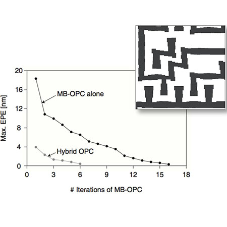
1. Improving conventional EDA SW (ML inside)
– Integrating ML-OPC with MB-OPC → 3~4 times speedup
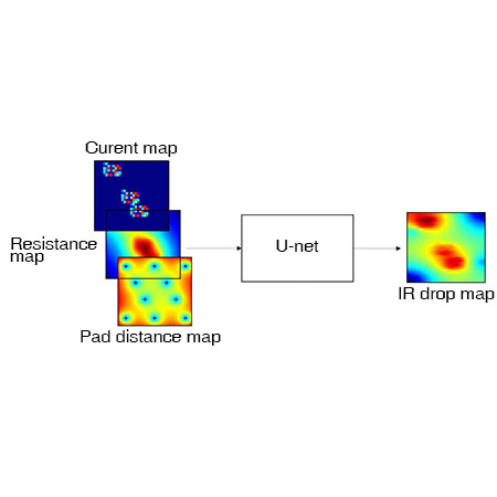
2. Replace conventional EDA SW (ML outside)
– ML-based IR drop analysis → ~20 times faster analysis
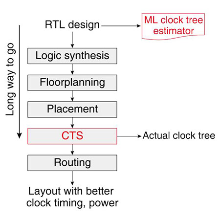
3. Late-stage design prediction from early-stage (ML around)
– Clock tree structure prediction from RTL-level
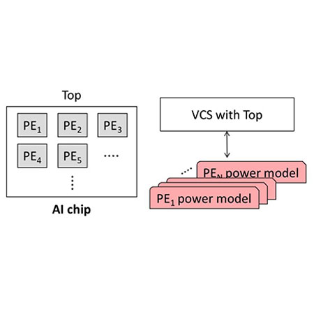
4. EDA for AI
– Fast power analysis of NPU by using single PE power model


Previous
Next
